EP0176685A2 - Method for detecting the digital sum variation of a serial data signal - Google Patents
Method for detecting the digital sum variation of a serial data signal Download PDFInfo
- Publication number
- EP0176685A2 EP0176685A2 EP85109251A EP85109251A EP0176685A2 EP 0176685 A2 EP0176685 A2 EP 0176685A2 EP 85109251 A EP85109251 A EP 85109251A EP 85109251 A EP85109251 A EP 85109251A EP 0176685 A2 EP0176685 A2 EP 0176685A2
- Authority
- EP
- European Patent Office
- Prior art keywords
- lds
- stage
- counter
- bit
- flip
- Prior art date
- Legal status (The legal status is an assumption and is not a legal conclusion. Google has not performed a legal analysis and makes no representation as to the accuracy of the status listed.)
- Ceased
Links
Images


Classifications
-
- H—ELECTRICITY
- H04—ELECTRIC COMMUNICATION TECHNIQUE
- H04L—TRANSMISSION OF DIGITAL INFORMATION, e.g. TELEGRAPHIC COMMUNICATION
- H04L25/00—Baseband systems
- H04L25/38—Synchronous or start-stop systems, e.g. for Baudot code
- H04L25/40—Transmitting circuits; Receiving circuits
- H04L25/49—Transmitting circuits; Receiving circuits using code conversion at the transmitter; using predistortion; using insertion of idle bits for obtaining a desired frequency spectrum; using three or more amplitude levels ; Baseband coding techniques specific to data transmission systems
- H04L25/4906—Transmitting circuits; Receiving circuits using code conversion at the transmitter; using predistortion; using insertion of idle bits for obtaining a desired frequency spectrum; using three or more amplitude levels ; Baseband coding techniques specific to data transmission systems using binary codes
- H04L25/4908—Transmitting circuits; Receiving circuits using code conversion at the transmitter; using predistortion; using insertion of idle bits for obtaining a desired frequency spectrum; using three or more amplitude levels ; Baseband coding techniques specific to data transmission systems using binary codes using mBnB codes
-
- G—PHYSICS
- G11—INFORMATION STORAGE
- G11B—INFORMATION STORAGE BASED ON RELATIVE MOVEMENT BETWEEN RECORD CARRIER AND TRANSDUCER
- G11B20/00—Signal processing not specific to the method of recording or reproducing; Circuits therefor
- G11B20/10—Digital recording or reproducing
- G11B20/14—Digital recording or reproducing using self-clocking codes
- G11B20/1403—Digital recording or reproducing using self-clocking codes characterised by the use of two levels
- G11B20/1423—Code representation depending on subsequent bits, e.g. delay modulation, double density code, Miller code
- G11B20/1426—Code representation depending on subsequent bits, e.g. delay modulation, double density code, Miller code conversion to or from block codes or representations thereof
Definitions
- the invention relates to a method for determining the current digital sum of a binary data signal.
- monitoring the transmission link during operation is of particular importance. Such monitoring is possible with the help of redundant line codes.
- the transmission quality can also be improved by a suitable choice of the code (for example by increasing the clock information, by improving the signal statistics and not least by error-correcting codes).
- Block codes with limited running digital sum are used for the transmission via fiber optic cables. Transmission errors lead to the limits of the LDS being exceeded. This provides an easy way to identify errors during operation. In the optical above wearing technology is used for line coding in general 5B6B code with the LDS limit of f 3.
- the present invention was therefore based on the object of specifying a method of the type mentioned at the outset, which enables an exact determination of the current digital
- the sum and possible exceeding of this LDS in the event of transmission errors is also permitted at very high transmission speeds.
- the method should be inexpensive and only require components that consume little power.
- Claims 2 and 3 represent advantageous refinements.
- Claims 4 to 10 identify optimal circuit arrangements for carrying out the method according to the invention.
- the claimed LDS method is very inexpensive to implement, with only a series / parallel converter, which of course must be designed on the input side for the high transmission speeds, a register with a width that enables the permitted states (with the 5B6B block code 7), and logic is required, this logic essentially having to perform comparison functions, namely a comparison between the data word supplied by the series / parallel converter with the last current LDS value, which is stored in the register, and a function to store the new LDSW value in the register based on the result of the comparison.
- FIG. 1 shows a state diagram for the LDS monitoring of 5B6B-coded signals which are divided into two partial data streams.
- FIG. 2 contains a block diagram for implementing LDS monitoring in accordance with the claimed method.
- the register content corresponds to the current value of the LDS and has the value 0. If the same bits arrive in pairs, the register content is then increased by two (at 1.1) or decreased (at 00).
- limit +3 When limit +3 is reached, bit patterns 11 and 10 each exceed the permissible range of +3 and are displayed as errors.
- the state of the register is also reduced by 1.
- the lower limit -3 the same applies analogously to the bit patterns 00 and 01, with the register content rising to -2 at 01.
- the two bit patterns 10 and 01 thus only lead to a change in the register content when the two limit values of +3 or -3 are reached, all other register states are not influenced by these two bit patterns.
- FIG. 3 shows a state diagram for the LDS monitoring of 5B6B-coded signals which are divided into two partial data streams.
- FIG. 4 shows a detailed block diagram for an embodiment of the circuit arrangement according to the invention.
- FIG. 5 shows a detailed circuit diagram for the arrangement according to FIG. 4 with a detailed resolution of logical combination and storage units.
- FIG. 6 shows a block circuit diagram for a 2-stage up-down counter with 4 cycles and
- FIG. 7 shows a detailed circuit diagram based on logical combination units for the same counter.
- FIG. 8 shows a variant for a counter according to FIG. 6 or 7, while FIG. 9 shows the logic combination diagram for a fast 2-stage up-down counter with 3 cycles.
- the state diagram of FIG. 3 does not differ from that of FIG. 1, it has only been drawn differently, so that 2 cycles, one with 3 states and the other with 4 states, can be seen. It is assumed that the register contents match the current value of the LDS and have the value 0. When the same bits arrive in pairs, the register content will change because increased by 2 (at 11) or decreased (at 00). When the limit +3 is reached, which causes a change from the 3 to the 4 cycle, the bit patterns 11 and 10, which returns the latter bit pattern to the 3 cycle, lead to the permissible range of +3 and being exceeded are displayed as errors. With the lower limit -3, the same applies analogously to the bit patterns 00 and 01, with the register content rising to -2 at 01. The two bit patterns 10 and 01 therefore only lead to a change in the register content when the two limit values of +3 or -3 are reached, all other register states are not influenced by these two bit patterns.
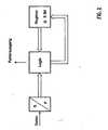
- a series-parallel converter S / P can be seen in FIG. generated by a divider stage 2: 1 divided clock T / 2 of 339 MHz.
- the two partial data streams S1 and S2 are fed to a coding logic which recognizes the 4 possible states of a bit pair S1 S2 and assigns them to an output.
- the decoding logic controls the LDS memory and an error logic.
- the LDS memory consists of 2 2-stage up / down counters, one running through the 3 states and the other through the 4 states cycle according to the state diagram according to FIG. 3.
- the two counters run up and down in parallel at half the clock frequency T / 2, and each stop automatically when the limit states +2, -2, +3, -3 are reached.
- the error logic compares the state of the counters with the output of the decoding logic.
- An error pulse generation downstream of the error logic generates an error pulse signal linked to the clock signal T / 2 for each error.
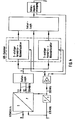
- the detailed circuit diagram according to FIG. 5 for the LDS circuit according to FIG. 4 provides logical logic and memory elements, which are advantageously implemented in ECL technology, which allow a maximum clock frequency of 880 MHz.
- the flip-flops are all master-slave D-flip-flops, while the logic gates are OR / NOR gates.
- the series-parallel converter comprises a 2-stage shift register, which consists of the two flip-flops FF1 and FF2 connected in series, and a 2-stage memory, which also consists of 2 flip-flops FF3 and FF4 and each with its inputs an output of the upstream shift register stages is connected.
- the shift register is clocked at the high clock rate T and thus generates 2 partial data streams of half the bit frequency from the serial data stream D present at the input of its first stage 'at its two outputs. These partial data streams are taken over by the 2-stage memory at half the clock frequency T / 2.
- the halved clock frequency is generated in a 5th, feedback flip-flop FF5 by dividing the high clock rate and distributed to the other modules of the LDS monitoring.
- the decoding logic consists of the 4 OR / NOR gates G1, G2, G3 and G4 with the outputs A, B, C, D and the inverted outputs ⁇ , and D.
- the decoding logic becomes the two partial data streams S1 and S2 or in inverted form Form ST, supplied and according to the following truth table 1
- the output signals of the decoding logic feed the two 2-stage up-down counters.
- the basic circuit diagram of such a counter is shown in FIG. 6.
- such a counter consists of a memory, which is controlled via a counter logic from the outside and from its output as feedback. It is clocked with the clock T / 2 and also has a stop input CE (Clock Enable).
- the signal for the clock enable input must be at least half a cycle long and must be present half a cycle before the clock edge.
- the control signals for the control for counting up and down must apply at least around the cycle times of the gate and around the set-up time, i.e. around 0.85 ns, before the clock edge.
- FIG. 7 A variant for realizing a fast up / down counter for the cycle of 4 is shown in FIG.
- This counter fulfills the same functions as the counter according to FIG. 7, except that one gate is saved, namely the internal OR operation in the second flip-flop stage B, and only one control line, namely ⁇ , is required.
- the purpose of the error logic is to generate an error pulse if the LDS exceeds the limits of ⁇ 3.
- the error logic contains logic gates G9 to G12, which match the bits received in pairs, which output the outputs of the decoding logic, with the states of the compare the counter.
- the positive clock edge is generated for another flip-flop FF10.
- the negative clock edge for this flip-flop is generated after its cycle time via a feedback from the output Q or from the inverted output Q of this flip-flop via further gates G18 and G19.
- the error pulse generation contains a further gate G21, with which the error signal described above is ORed with the error pulse of the flip-flop FF10.
- the output signal of the gate G21 is linked in a further gate G22 with the operating clock T / 2, so that a pulse of a defined duration is present at the output of this gate for each error.
Abstract
Description
Die Erfindung betrifft ein Verfahren zur Ermittlung der laufenden digitalen Summe-eines binären Datensignals. In digitalen Übertragungssystemen großer Übertragungskapazität kommt der Überwachung der übertragungsstrecke während des laufenden Betriebs besondere Bedeutung zu. Mit Hilfe von redundanten Leitungscodes ist eine derartige Überwachung möglich. Darüberhinaus kann durch geeignete Wahl des Codes auch die Übertragungsqualität verbessert werden (beispielsweise durch Erhöhung der Taktinformation, durch Verbesserung der Signalstatistik und nicht zuletzt durch fehlerkorrigierende Codes).The invention relates to a method for determining the current digital sum of a binary data signal. In digital transmission systems with a large transmission capacity, monitoring the transmission link during operation is of particular importance. Such monitoring is possible with the help of redundant line codes. In addition, the transmission quality can also be improved by a suitable choice of the code (for example by increasing the clock information, by improving the signal statistics and not least by error-correcting codes).
Für die Übertragung über Lichtwellenleiter werden Blockcodes mit begrenzter laufender digitaler Summe eingesetzt (LDS). Fehler der Übertragung führen zum Überschreiten der Grenzen der LDS. Damit ist eine einfache Möglichkeit zur Fehlererkennung während des Betriebs gegeben. In der optischen übertragungstechnik wird für die Leitungscodierung im allgemeinen 5B6B-Code mit der LDS-Grenze von f3 verwendet.Block codes with limited running digital sum (LDS) are used for the transmission via fiber optic cables. Transmission errors lead to the limits of the LDS being exceeded. This provides an easy way to identify errors during operation. In the optical above wearing technology is used for line coding in general 5B6B code with the LDS limit of f 3.
In dem Aufsatz "Leitungscodierung und betriebliche überwachung bei regenerativen Lichtleitkabel-Übertragungssyste- men" von Drullmann und Kammerer in Frequenz 34, 1980, Nr. 2, Seite 45 ff. ist ein Verfahren der eingangs genannten Art beschrieben. Es sind auch Schaltungsanordnungen zur Realisierung dieses Verfahrens angegeben, zum einen einen digitalen LDS-Zähler und zum anderen eine analoge Schaltungsanordnung mittels Integrator zur Fehlererkennung. In dem Aufsatz werden die beiden Schaltungen diskutiert, wobei auf den hohen Aufwand an Digitalschaltkreisen sowie auf die verhältnismäßig hohe Leistungsaufnahme der Schaltung hingewiesen wird. Die analoge Fehlererkennungsschaltung weist einen vertretbaren Schaltungsaufwand bei vergleichsweise geringer Leistungsaufnahme auf. Bei beiden Schaltungen muß jedochIn the article "line coding and operational supervision in regenerative light pipe Übertragungssyste - men" of Drullmann and Kammerer in frequency 34, 1980, No. 2, page 45 et seq, a method of the type mentioned described... Circuit arrangements for realizing this method are also specified, on the one hand a digital LDS counter and on the other hand an analog circuit arrangement by means of an integrator for error detection. The two circuits are discussed in the article, with reference being made to the high expenditure on digital circuits and to the relatively high power consumption of the circuit. The analog error detection circuit has a reasonable circuit outlay with a comparatively low power consumption. In both circuits, however
bei jedem empfangenen Bit entschieden werden, in welcher Weise der Zähler bzw. der Integratorzustand geändert werden muß. Bei sehr hohen übertragungsgeschwindigkeiten steht für diese Entscheidung nur eine entsprechend kurze Zeit zur Verfügung, was zu erheblichen Schwierigkeiten führen kann, wenn diese Zeit, die der Taktzeit des übertragungssystems entspricht, in die Grössenordnung der Durchlaufzeiten der für die Fehlererkennung verwendeten Schaltkreise kommt. Zusätzlich ist bei der analogen Fehlererkennungsschaltung ein Monoflop vorgesehen, das eine erste Fehlüberschreitung soweit verlängert, bis auch die zweite Überschreitung mit hoher Wahrscheinlichkeit stattgefunden hat. Eine solche Schaltungsfunktion kann nicht die Grundlage einer genauen Ermittlung der üübertragungsfehlerrate sein.for each bit received, a decision is made as to how the counter or the integrator state must be changed. At very high transmission speeds, there is only a correspondingly short time available for this decision, which can lead to considerable difficulties if this time, which corresponds to the cycle time of the transmission system, is in the order of magnitude of the throughput times of the circuits used for error detection. In addition, a monoflop is provided in the analog error detection circuit, which extends a first overshoot until the second overshoot has also occurred with high probability. Such a circuit function cannot be the basis for an exact determination of the transmission error rate.
Der vorliegenden Erfindung lag deshalb die Aufgabe zugrunde, ein Verfahren der eingangs genannten Art anzugeben, das eine exakte Ermittlung der laufenden digitalen Summe und eine etwaige Überschreitung dieser LDS bei Übertragungsfehlern auch bei sehr hohen übertragungsgeschwindigkeiten gestattet. Das Verfahren soll aufwandsgünstig sein und nur solche Bauelemente erforderlich machen, die wenig Leistung aufnehmen.The present invention was therefore based on the object of specifying a method of the type mentioned at the outset, which enables an exact determination of the current digital The sum and possible exceeding of this LDS in the event of transmission errors is also permitted at very high transmission speeds. The method should be inexpensive and only require components that consume little power.
Die Lösung erfolgt durch die im Anspruch 1 gekennzeichneten Merkmale.The solution is achieved by the features characterized in
Die Ansprüche 2 und 3 geben vorteilhafte Ausgestaltungen wieder. Die Ansprüche 4 bis 10 kennzeichnen optimale Schaltungsanordnungen zur.Durchführung des erfindungsgemäßen Verfahrens.
In der deutschen Patentanmeldung P 34 08 646.3 (BK 83/131) ist eine Schaltungsanordnung ebenfalls zum Ermitteln und überwachen der LDS gemäß der eingangs genannten Art vorgeschlagen worden. Diese Anordnung weist eine aufwandsgünstige Realisierung mit wenig Schaltungsaufwand und geringer Verlustleistung auf, es gelten hier jedoch die gleichen Schwierigkeiten, wenn die Taktzeit der Übertragungseinrichtung in die Größenordnung der Durchlaufzeit der in dieser Schaltung verwendeten Flip-Flops kommt.In the German patent application P 34 08 646.3 (BK 83/131) a circuit arrangement has also been proposed for determining and monitoring the LDS in accordance with the type mentioned at the beginning. This arrangement has a cost-effective implementation with little circuit complexity and low power dissipation, but the same difficulties apply here if the cycle time of the transmission device comes in the order of the throughput time of the flip-flops used in this circuit.
Durch die Umwandlung des seriellen Datenstromes in mehrere gleichlangsame Teildatenströme ergibt sich der Vorteil einer dem Teilungsfaktor entsprechenden Verkleinerung der Verarbeitungsgeschwindigkeit. Infolgedessen kann die LDS-Realisierung mit wesentlich langsameren Bausteinen erfolgen. Oder anders ausgedrückt, eine LDS-Realisierung ist auch für höchste Übertragungsfrequenzen machbar und weist eine sichere Betriebsfunktion auf. Das beanspruchte LDS-Verfahren ist sehr aufwandsgünstig zu realisieren, wobei lediglich ein Serien-/Parallelwandler, der natürlich eingangsseitig für die hohen Übertragungsgeschwindigkeiten ausgebildet sein muß, ein Register mit einer Breite, welche es ermöglicht, die erlaubten Zustände (beim 5B6B-Blockcode 7) zu speichern, sowie eine Logik erforderlich ist, wobei diese Logik im wesentlichen Vergleichsfunktionen durchzuführen hat, nämlich einen Vergleich zwischen dem von dem Serien-/Parallelwandler gelieferten Datenwort mit dem letzten aktuellen LDS-Wert, der im Register gespeichert ist, sowie eine Funktion zum Einspeichern des neuen LDSW-Wertes in das Register aufgrund des Ergebnisses der Vergleichs.The conversion of the serial data stream into several equally slow partial data streams results in the advantage of a reduction in the processing speed corresponding to the division factor. As a result, LDS implementation can be done with much slower modules. In other words, an LDS implementation is also feasible for the highest transmission frequencies and has a safe operating function. The claimed LDS method is very inexpensive to implement, with only a series / parallel converter, which of course must be designed on the input side for the high transmission speeds, a register with a width that enables the permitted states (with the 5B6B block code 7), and logic is required, this logic essentially having to perform comparison functions, namely a comparison between the data word supplied by the series / parallel converter with the last current LDS value, which is stored in the register, and a function to store the new LDSW value in the register based on the result of the comparison.
Es folgt nun eine Beschreibung der Erfindung anhand der Figuren.There now follows a description of the invention with reference to the figures.
Die Figur 1 zeigt ein Zustandsdiagramm für die LDS-Überwachung von 5B6B-codierten Signalen, die in zwei Teildatenströme aufgeteilt werden.FIG. 1 shows a state diagram for the LDS monitoring of 5B6B-coded signals which are divided into two partial data streams.
Die Figur 2 enthält ein Blockschaltbild zur Realisierung einer LDS-Überwachung gemäß dem beanspruchten Verfahren. In Figur 1 sei angenommen, daß der Registerinhalt mit dem aktuellen Wert der LDS übereinstimme und den Wert 0 aufweise. Bei Eintreffen von paarweise gleichen Bits wird der Registerinhalt dann jeweils um zwei erhöht (bei 1.1) oder erniedrigt (bei 00). Bei Erreichen der Grenze +3 führen die Bitmuster 11 und 10 jeweils zur Überschreitung des zulässigen Bereichs von +3 und werden als Fehler angezeigt. Bei dem Bitmuster 10 wird außerdem der Zustand des Registers um 1 verringert. Bei der unteren Grenze -3 gilt sinngemäß das gleiche für die Bitmuster 00 und 01, wobei bei 01 der Registerinhalt auf -2 ansteigt. Die beiden Bitmuster 10 und 01 führen also lediglich, wenn die beiden Grenzwerte von +3 bzw. -3 erreicht sind, zu einer Änderung des Registerinhaltes, alle anderen Registerzustände werden von diesen beiden Bitmustern nicht beeinflußt.FIG. 2 contains a block diagram for implementing LDS monitoring in accordance with the claimed method. In FIG. 1 it is assumed that the register content corresponds to the current value of the LDS and has the
Sofern die Übertragungsgeschwindigkeit so hohe Werte aufweist, daß eine Halbierung des Datenstromes und damit eine Halbierung der Verarbeitungsgeschwindigkeit immer noch nicht ausreichend ist, kann eine weitere Parallelisierung des Empfangssignals, d.h. eine Erhöhung von n über 2 hinaus selbstverständlich durchgeführt werden, wodurch eine entsprechend weitere Reduzierung der Verarbeitungsgeschwindigkeit erreicht wird. Allerdings ist dann der Aufwand für die Serien-/Parallelwandlung und für die Logik (aufgrund des breiteren Wortes) geringfügig höher.If the transmission speed has such high values that the data stream is halved and thus the processing speed is halved is not sufficient, a further parallelization of the received signal, ie an increase of n beyond 2 can of course be carried out, whereby a corresponding further reduction in the processing speed is achieved. However, the effort for the serial / parallel conversion and for the logic (due to the broader word) is slightly higher.
Die Figur 3 zeigt ein Zustandsdiagramm für die LDS-Überwachung von 5B6B-codierten Signalen, die in 2 Teildatenströme aufgeteilt werden.FIG. 3 shows a state diagram for the LDS monitoring of 5B6B-coded signals which are divided into two partial data streams.
Die Figur 4 stellt ein detailliertes Blockschaltbild für eine Ausführungsform der erfindungsgemäßen Schaltungsanordnung dar.FIG. 4 shows a detailed block diagram for an embodiment of the circuit arrangement according to the invention.
In Figur 5 schließlich ist ein detailliertes Schaltbild für die Anordnung nach Figur 4 mit einer Detailauflösung von logischen Verknüpfungs- und Speichereinheiten wiedergegeben.Finally, FIG. 5 shows a detailed circuit diagram for the arrangement according to FIG. 4 with a detailed resolution of logical combination and storage units.
Die Figur 6 zeigt ein Blockschaltbild für einen 2-stufigen Vor- Rückwärtszähler mit 4 Zyklen und Bild 7 einen detaillierten Schaltplan auf der Grundlage von logischen Verknüpfungseinheiten für den selben Zähler.FIG. 6 shows a block circuit diagram for a 2-stage up-down counter with 4 cycles and FIG. 7 shows a detailed circuit diagram based on logical combination units for the same counter.
Die Figur 8 gibt eine Variante für einen Zähler gemäß Figur 6 oder 7 wieder, während Figur 9 den logischen Verknüpfungsschaltplan für einen schnellen 2-stufigen Vor- Rückwärtszähler mit 3 Zyklen wiedergibt.FIG. 8 shows a variant for a counter according to FIG. 6 or 7, while FIG. 9 shows the logic combination diagram for a fast 2-stage up-down counter with 3 cycles.
Das Zustandsdiagramm der Figur 3 unterscheidet sich nicht von demjenigen der Figur 1, es wurde lediglich anders gezeichnet, so daß 2 Zyklen, der eine mit 3 Zuständen und der andere mit 4 Zuständen, erkennbar werden. Es sei angenommen, daß der Registerinhalt mit dem aktuellen Wert der LDS übereinstimme und den Wert 0 aufweise. Bei Eintreffen von paarweise gleichen Bits wird der Registerinhalt dann jeweils um 2 erhöht (bei 11) oder erniedrigt (bei 00). Bei Erreichen der Grenze +3, wodurch ein Wechsel vom 3-er zum 4-er Zyklus stattfindet, führen die Bitmuster 11 und 10, welch letzteres Bitmuster wieder zurückführt in den 3-er Zyklus, jeweils zur Überschreitung des zulässigen Bereichs von +3 und werden als Fehler angezeigt. Bei der unteren Grenze -3 gilt sinngemäß das gleiche für die Bitmuster 00 und 01, wobei bei 01 der Registerinhalt auf -2 ansteigt. Die beiden Bitmuster 10 und 01 führen also lediglich, wenn die beiden Grenzwerte von +3 bzw. -3 erreicht sind, zu einer Änderung des Registerinhaltes, alle anderen Registerzustände werden von diesen beiden Bitmustern nicht beeinflußt.The state diagram of FIG. 3 does not differ from that of FIG. 1, it has only been drawn differently, so that 2 cycles, one with 3 states and the other with 4 states, can be seen. It is assumed that the register contents match the current value of the LDS and have the
In Figur 4 ist ein Serien-Parallel-Wandler S/P erkennbar, welcher aus dem seriell mit 678 MBit/s einlaufenden Datensignal D 2 Teildatenströme von 339 MBit/s S1 und S2 unter Zuhilfenahme des eingangsseitigen Taktes von 678 MHz und des ausgangsseitig verwendeten, durch eine Teilerstufe 2:1 geteilten Taktes T/2 von 339 MHz erzeugt. Die beiden Teildatenströme S1 und S2 werden einer Codierlogik zugeführt, welche die 4 möglichen Zustände jeweils eines Bitpaares S1 S2 erkennt und jeweils einem Ausgang zuordnet. Durch die Decodierlogik werden der LDS-Speicher und eine Fehlerlogik angesteuert. Der LDS-Speicher besteht aus 2 2-stufigen Vor- Rückwärtszählern, wobei der eine den 3 Zustände und der andere den 4 Zustände umfassenden Zyklus gemäß Zustandsdiagramm nach Fig. 3 durchläuft. Die beiden Zähler laufen parallel mit der halben Taktfrequenz T/2 auf- bzw. abwärts, wobei sie bei Erreichen der Grenzzustände +2, -2, +3, -3 jeweils selbständig anhalten. Durch die Fehlerlogik wird der Zustand der Zähler mit dem Ausgang der Decodierlogik verglichen. Eine der Fehlerlogik nachgeschaltete Fehlerimpulserzeugung erzeugt für jeden Fehler ein mit dem Taktsignal T/2 verknüpftes Fehlerimpulssignal.A series-parallel converter S / P can be seen in FIG. generated by a divider stage 2: 1 divided clock T / 2 of 339 MHz. The two partial data streams S1 and S2 are fed to a coding logic which recognizes the 4 possible states of a bit pair S1 S2 and assigns them to an output. The decoding logic controls the LDS memory and an error logic. The LDS memory consists of 2 2-stage up / down counters, one running through the 3 states and the other through the 4 states cycle according to the state diagram according to FIG. 3. The two counters run up and down in parallel at half the clock frequency T / 2, and each stop automatically when the limit states +2, -2, +3, -3 are reached. The error logic compares the state of the counters with the output of the decoding logic. An error pulse generation downstream of the error logic generates an error pulse signal linked to the clock signal T / 2 for each error.
Der detaillierte Stromlaufplan gemäß Figur 5 für die LDS-Schaltung nach Figur 4 sieht logische Verknüpfungs- und Speicherelemente vor, die vorteilhafterweise in ECL-Technik ausgeführt sind, welche eine maximale Taktfrequenz von 880 MHz zulassen. Die Flip-Flops sind durchweg Master-Slave D-Flip-Flops, während die Verknüpfungsglieder OR/NOR-Glieder sind.The detailed circuit diagram according to FIG. 5 for the LDS circuit according to FIG. 4 provides logical logic and memory elements, which are advantageously implemented in ECL technology, which allow a maximum clock frequency of 880 MHz. The flip-flops are all master-slave D-flip-flops, while the logic gates are OR / NOR gates.
Der Serien-Parallel-Wandler umfaßt ein 2-stufiges Schieberegister, das aus den beiden hintereinandergeschalteten Flip-Flop FF1 und FF2 besteht, und einen 2-stufigen Speicher, der ebenfalls aus 2 Flip-Flops FF3 und FF4 besteht und mit seinen Eingängen jeweils mit einem Ausgang der vorgeschalteten Schieberegisterstufen verbunden ist. Das Schieberegister wird mit der hohen Taktrate T getaktet und erzeugt somit aus dem am Eingang seiner ersten Stufe' anstehenden seriellen Datenstrom D an seinen beiden Ausgängen 2 Teildatenströme der halben Bitfrequenz. Diese Teildatenströme werden mit der halben Taktfrequenz T/2 von dem 2-stufigen Speicher übernommen. Die halbierte Taktfrequenz wird in einem 5., rückgekoppelten Flip-Flop FF5 durch Teilung der hohen Taktrate erzeugt und an die übrigen Baugruppen der LDS-Überwachung verteilt.The series-parallel converter comprises a 2-stage shift register, which consists of the two flip-flops FF1 and FF2 connected in series, and a 2-stage memory, which also consists of 2 flip-flops FF3 and FF4 and each with its inputs an output of the upstream shift register stages is connected. The shift register is clocked at the high clock rate T and thus generates 2 partial data streams of half the bit frequency from the serial data stream D present at the input of its first stage 'at its two outputs. These partial data streams are taken over by the 2-stage memory at half the clock frequency T / 2. The halved clock frequency is generated in a 5th, feedback flip-flop FF5 by dividing the high clock rate and distributed to the other modules of the LDS monitoring.
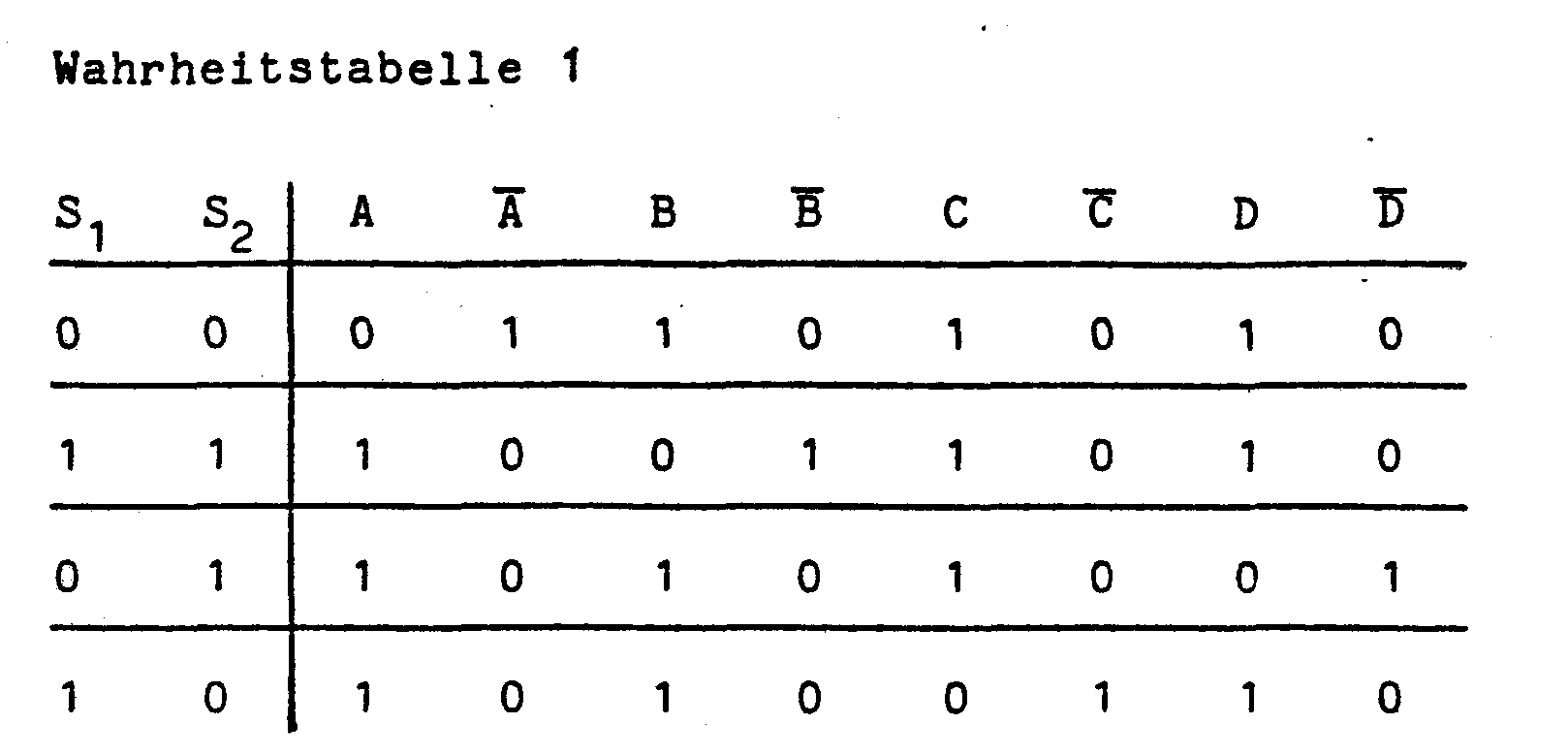
Die Decodierlogik besteht aus den 4 OR/NOR-Gliedern G1, G2, G3 und G4 mit den Ausgängen A, B, C, D und den invertierten Ausgängen Ä, und D. Der Decodierlogik werden die beiden Teildatenströme S1 und S2 bzw. in invertierter Form ST, zugeführt und nach folgender Wahrheitstabelle 1

verarbeitet.-Diese Wahrheitstabelle entspricht den folgenden logischen Verknüpfungsvorschriften![]()
![]()
![]()
![]()
![]()
![]()
![]()
![]()
Die Ausgangssignale der Decodierlogik speisen die beiden 2-stufigen Vor- Rückwärtszähler. Das Prinzipschaltbild eines solchen Zählers ist in Figur 6 dargestellt. Im Prinzip besteht ein solcher Zähler aus einem Speicher, der über eine Zähllogik von außen und von seinem Ausgang als Rückkopplung angesteuert wird. Er wird mit dem Takt T/2 getaktet und verfügt außerdem über einen Stop-Eingang CE (Clock Enable).The output signals of the decoding logic feed the two 2-stage up-down counters. The basic circuit diagram of such a counter is shown in FIG. 6. In principle, such a counter consists of a memory, which is controlled via a counter logic from the outside and from its output as feedback. It is clocked with the clock T / 2 and also has a stop input CE (Clock Enable).
Der Figur 5 und noch detaillierter der Figur 7 ist der lo- 'gische Schaltplan eines 2-stufigen Vor- Rückwärtszählers für den 4-er Zyklus mit Grenzzustandserkennung entnehmbar. Die beiden Stufen enthalten jeweils ein Flip-Flop als Speicher FF6 und FF7, die über je 2 NOR-Glieder G5, G6, G7 und G8 angesteuert werden. Der Zählereingang wird mit den Decodierlogik-Ausgangssignalen A bzw. ? beaufschlagt. Der Zähler arbeitet nach der folgenden Wahrheitstabelle 2

- Propagation Delay FF : 1,0 ns
- Set-up Time FF : 0,1 ns
- Propagation Delay Gatter: 0,75 ns
- Laufzeit durch Leitungen: 0,1 ns
- Propagation Delay FF: 1.0 ns
- Set-up time FF: 0.1 ns
- Propagation delay gate: 0.75 ns
- Running time through lines: 0.1 ns
Das ergibt eine maximale Zählfrequenz von etwa 513 MHz. Bei den Setzeingängen ist zu beachten, daß für den Clock-Enable-Eingang das Signal mindestens eine halbe Taktdauer lang sein muß und eine halbe Taktdauer vor der Taktflanke anliegen muß. Die Steuersignale zur Steuerung für Vor- und Rückwärtszählen müssen mindestens um die Durchlaufzeiten des Gatters und um die Set-up Time, also etwa um 0,85 ns, vor der Taktflanke anlegen.This results in a maximum counting frequency of around 513 MHz. With the set inputs, it should be noted that the signal for the clock enable input must be at least half a cycle long and must be present half a cycle before the clock edge. The control signals for the control for counting up and down must apply at least around the cycle times of the gate and around the set-up time, i.e. around 0.85 ns, before the clock edge.
Eine Variante zur Realisierung eines schnellen Vor- Rückwärtszählers für den 4er-Zyklus ist in Figur 8 dargestellt. Dieser Zähler erfüllt die gleichen Funktionen wie der Zähler nach Figur 7, wobei jedoch ein Gatter eingespart wird, nämlich die interne OR-Verknüpfung in der 2. Flip-Flop-Stufe B, und wobei nur eine Steuerleitung, nämlich Ä, benötigt wird.A variant for realizing a fast up / down counter for the cycle of 4 is shown in FIG. This counter fulfills the same functions as the counter according to FIG. 7, except that one gate is saved, namely the internal OR operation in the second flip-flop stage B, and only one control line, namely Ä, is required.
Der 2-stufige Vor- Rückwärtszähler für den 3er-Zyklus ist ebenfalls aus Figur 5 und etwas detaillierter aus Figur 9 entnehmbar, er besteht aus den beiden Flip-Flop-Stufen FF8 und FF9 und realisiert die rechte Hälfte des Zustandsdiagramms gemäß Figur 3. Der Zähler besitzt 2 Steuereingänge B und B, die wie die beiden invertierten Ausgänge der Zählerstufen über die internen ODER-Gatter auf ihre beiden direkten Setzeingänge wirken. Der Zähler arbeitet nach der folgenden Wahrheitstabelle 3

- Propagation Delay FF : 1,0 ns
- Set-up Time FF : 0,1 ns
- Laufzeit durch Leitungen : 0,1 ns.
- Propagation Delay FF: 1.0 ns
- Set-up time FF: 0.1 ns
- Running time through lines: 0.1 ns.
Daraus ergibt sich eine maximale Zählfrequenz von etwa 830 MHz. Zu beachten ist hier, daß die Steuersignale zur Steuerung für Vor- Rückwärtszählen lediglich um die Set-up Time versetzt vor der Taktflanke, also um 0,1 ns früher, anliegen müssen.This results in a maximum counting frequency of around 830 MHz. It should be noted here that the control signals for the control for counting downwards only have to be applied offset by the set-up time before the clock edge, that is, 0.1 ns earlier.
Die Fehlerlogik hat die Aufgabe, einen Fehlerimpuls zu erzeugen, wenn die LDS die Grenzen von ±3 überschreitet. Wie aus dem Zustandsdiagramm der Figur 3 zu erkennen ist, wirkt sich ein Wechsel zwischen den Zählern wie eine Überschreitung der Grenzen der LDS aus. Darüber hinaus führen die Bit-Kombinationen 00 bei der Zählerstellung -3 und 11 bei der Zählerstellung +3 ebenfalls zur Überschreitung der LDS. Die Fehlerlogik enthält logisches Verknüpfungsgatter G9 bis G12, welche die paarweise empfangenen Bits, welche die Ausgänge der Decodierlogik abgeben, mit den Zuständen der beiden Zähler vergleichen. Beim Übergang zwischen den Zählern wird die positive Taktflanke für ein weiteres Flip-Flop FF10 erzeugt. über eine Rückkopplung vom Ausgang Q bzw. vom invertierten Ausgang Q dieses Flip-Flops über weitere Gatter G18 und G19 wird die negative Taktflanke für dieses Flip-Flop nach seiner Durchlaufzeit erzeugt. Wenn zwischen den Zählern umgeschaltet wird, liegt somit am Takteingang des Flip-Flops FF10 ein Impuls, dessen Dauer von den Laufzeiten in der Rückkopplung bestimmt ist. Mit Hilfe des Gatters G6 und weiterer Gatter G13, G16, G17 und G20 wird beim Zustand ±3 des Zählers erkannt, ob die Bit-Kombinationen 00 bzw. 11 am Eingang anliegen.The purpose of the error logic is to generate an error pulse if the LDS exceeds the limits of ± 3. As can be seen from the state diagram in FIG. 3, a change between the counters has the effect of exceeding the limits of the LDS. In addition, the
Die Fehlerimpulserzeugung enthält ein weiteres Gatter G21, mit dem eine ODER-Verknüpfung des weiter oben beschriebenen Fehlersignals mit dem Fehlerimpuls des Flip-Flops FF10 durchgeführt wird. Das Ausgangssignal des Gatters G21 wird in einem weiteren Gatter G22 mit dem Betriebstakt T/2 verknüpft, so daß am Ausgang dieses Gatters für jeden Fehler ein Impuls definierter Dauer ansteht.The error pulse generation contains a further gate G21, with which the error signal described above is ORed with the error pulse of the flip-flop FF10. The output signal of the gate G21 is linked in a further gate G22 with the operating clock T / 2, so that a pulse of a defined duration is present at the output of this gate for each error.
Claims (10)


Applications Claiming Priority (4)
| Application Number | Priority Date | Filing Date | Title |
|---|---|---|---|
| DE3434852 | 1984-09-22 | ||
| DE19843434852 DE3434852A1 (en) | 1984-09-22 | 1984-09-22 | Method for determining the running digital sum of a serial data signal |
| DE19853505704 DE3505704A1 (en) | 1985-02-19 | 1985-02-19 | Circuit arrangement for determining and monitoring the running digital sum (RDS) |
| DE3505704 | 1985-02-19 |
Publications (2)
| Publication Number | Publication Date |
|---|---|
| EP0176685A2 true EP0176685A2 (en) | 1986-04-09 |
| EP0176685A3 EP0176685A3 (en) | 1988-08-03 |
Family
ID=25824990
Family Applications (1)
| Application Number | Title | Priority Date | Filing Date |
|---|---|---|---|
| EP85109251A Ceased EP0176685A3 (en) | 1984-09-22 | 1985-07-24 | Method for detecting the digital sum variation of a serial data signal |
Country Status (1)
| Country | Link |
|---|---|
| EP (1) | EP0176685A3 (en) |
Cited By (2)
| Publication number | Priority date | Publication date | Assignee | Title |
|---|---|---|---|---|
| EP0250049A1 (en) * | 1986-06-20 | 1987-12-23 | Koninklijke Philips Electronics N.V. | Channel encoder |
| EP1244220A2 (en) * | 2001-03-24 | 2002-09-25 | Lg Electronics Inc. | Method for modulating digital data and apparatus therefor |
Citations (3)
| Publication number | Priority date | Publication date | Assignee | Title |
|---|---|---|---|---|
| US3810111A (en) * | 1972-12-26 | 1974-05-07 | Ibm | Data coding with stable base line for recording and transmitting binary data |
| FR2504755A1 (en) * | 1981-04-24 | 1982-10-29 | Sony Corp | METHOD AND APPARATUS FOR ENCODING DIGITAL SIGNAL WITHOUT REVERSE ZERO RETURN WITH LOW CONTINUOUS COMPONENT |
| DE3235814A1 (en) * | 1982-09-28 | 1984-03-29 | Siemens AG, 1000 Berlin und 8000 München | Circuit arrangement for recoding a binary digital information flow into an nB/(n+1) B line code |
-
1985
- 1985-07-24 EP EP85109251A patent/EP0176685A3/en not_active Ceased
Patent Citations (3)
| Publication number | Priority date | Publication date | Assignee | Title |
|---|---|---|---|---|
| US3810111A (en) * | 1972-12-26 | 1974-05-07 | Ibm | Data coding with stable base line for recording and transmitting binary data |
| FR2504755A1 (en) * | 1981-04-24 | 1982-10-29 | Sony Corp | METHOD AND APPARATUS FOR ENCODING DIGITAL SIGNAL WITHOUT REVERSE ZERO RETURN WITH LOW CONTINUOUS COMPONENT |
| DE3235814A1 (en) * | 1982-09-28 | 1984-03-29 | Siemens AG, 1000 Berlin und 8000 München | Circuit arrangement for recoding a binary digital information flow into an nB/(n+1) B line code |
Non-Patent Citations (2)
| Title |
|---|
| IBM TECHNICAL DISCLOSURE BULLETIN, Band 21, Nr. 4, September 1978, Seiten 1600-1604, New York, US; J.A. ROONEY: "Encoding scheme with no clock transitions and restricted accumulated DC content" * |
| IBM TECHNICAL DISCLOSURE BULLETIN, Band 22, Nr. 5, Oktober 1979, Seiten 2025-2032, New York, US; J.A. ROONEY: "Improved rate 6/8(0,3) code and implementation" * |
Cited By (3)
| Publication number | Priority date | Publication date | Assignee | Title |
|---|---|---|---|---|
| EP0250049A1 (en) * | 1986-06-20 | 1987-12-23 | Koninklijke Philips Electronics N.V. | Channel encoder |
| EP1244220A2 (en) * | 2001-03-24 | 2002-09-25 | Lg Electronics Inc. | Method for modulating digital data and apparatus therefor |
| EP1244220A3 (en) * | 2001-03-24 | 2004-07-28 | Lg Electronics Inc. | Method for modulating digital data and apparatus therefor |
Also Published As
| Publication number | Publication date |
|---|---|
| EP0176685A3 (en) | 1988-08-03 |
Similar Documents
| Publication | Publication Date | Title |
|---|---|---|
| DE2608902C3 (en) | Code converter device | |
| CH620068A5 (en) | ||
| DE2320422A1 (en) | PROCEDURE FOR ERROR DETECTION | |
| DE3022746A1 (en) | DIGITAL PHASE COMPARATOR CIRCUIT | |
| EP0033565A2 (en) | Adaptive delta modulator | |
| EP0003480A2 (en) | Circuit for converting binary information by means of check bits | |
| DE2618633C3 (en) | PCM decoder | |
| DE2158548A1 (en) | Regenerative booster for digital transmission systems | |
| DE2704756C2 (en) | Digital-to-analog converter | |
| DE2937777C2 (en) | Control device in an electronic data processing system for program interruption and for performing forced operations | |
| EP0176685A2 (en) | Method for detecting the digital sum variation of a serial data signal | |
| CH671127A5 (en) | ||
| DE2849001C2 (en) | Network for adaptive delta modulation | |
| DE3822324A1 (en) | DEVICE FOR DISASSEMBLING THE PRIORITY VALUE | |
| DE3505704C2 (en) | ||
| DE1292183B (en) | Circuit arrangement for phase correction of signals emitted by a clock generator by means of pulse-shaped control signals | |
| DE3444315A1 (en) | Fast nB/mB coder | |
| DE2525533C2 (en) | Device for decoding a code | |
| EP0004341B1 (en) | Synchronisation of a local oscillator with a reference oscillator | |
| DE3021485C2 (en) | Method and circuit arrangement for carrier frequency monitoring in a communication system | |
| DE3310713C2 (en) | ||
| CH647366A5 (en) | CODING DEVICE FOR BINARY DATA SIGNALS AND DECODING DEVICE FOR THESE DATA SIGNALS. | |
| DE2339007C2 (en) | Method and circuit arrangement for inserting synchronization signals | |
| DE1925915A1 (en) | Converter | |
| DE2339026C2 (en) | Method and circuit arrangement for removing parity bits from binary words |
Legal Events
| Date | Code | Title | Description |
|---|---|---|---|
| PUAI | Public reference made under article 153(3) epc to a published international application that has entered the european phase |
Free format text: ORIGINAL CODE: 0009012 |
|
| AK | Designated contracting states |
Kind code of ref document: A2 Designated state(s): FR GB IT |
|
| PUAL | Search report despatched |
Free format text: ORIGINAL CODE: 0009013 |
|
| AK | Designated contracting states |
Kind code of ref document: A3 Designated state(s): FR GB IT |
|
| 17P | Request for examination filed |
Effective date: 19880831 |
|
| 17Q | First examination report despatched |
Effective date: 19900115 |
|
| STAA | Information on the status of an ep patent application or granted ep patent |
Free format text: STATUS: THE APPLICATION HAS BEEN REFUSED |
|
| 18R | Application refused |
Effective date: 19900630 |
|
| RIN1 | Information on inventor provided before grant (corrected) |
Inventor name: SALVASOHN, MANFRED, DIPL.-ING. Inventor name: KREMERS, ERNST, DIPL.-ING. |