4-STAGE PRESETTABLE RIPPLE COUNTERS SN54/74LS196 ...
4-STAGE PRESETTABLE RIPPLE COUNTERS SN54/74LS196 ...
4-STAGE PRESETTABLE RIPPLE COUNTERS SN54/74LS196 ...

You also want an ePaper? Increase the reach of your titles
YUMPU automatically turns print PDFs into web optimized ePapers that Google loves.
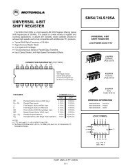
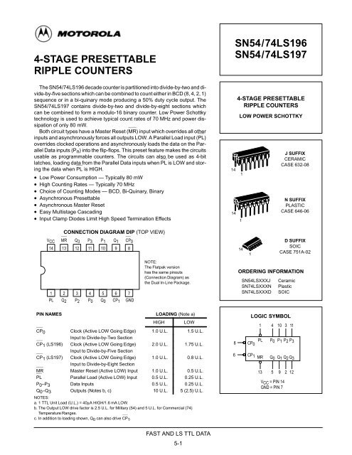
4-<strong>STAGE</strong> <strong>PRESETTABLE</strong><strong>RIPPLE</strong> <strong>COUNTERS</strong>The <strong>SN54</strong>/<strong>74LS196</strong> decade counter is partitioned into divide-by-two and divide-by-fivesections which can be combined to count either in BCD (8, 4, 2, 1)sequence or in a bi-quinary mode producing a 50% duty cycle output. The<strong>SN54</strong>/74LS197 contains divide-by-two and divide-by-eight sections whichcan be combined to form a modulo-16 binary counter. Low Power Schottkytechnology is used to achieve typical count rates of 70 MHz and power dissipationof only 80 mW.Both circuit types have a Master Reset (MR) input which overrides all otherinputs and asynchronously forces all outputs LOW. A Parallel Load input (PL)overrides clocked operations and asynchronously loads the data on the ParallelData inputs (Pn) into the flip-flops. This preset feature makes the circuitsusable as programmable counters. The circuits can also be used as 4-bitlatches, loading data from the Parallel Data inputs when PL is LOW and storingthe data when PL is HIGH.• Low Power Consumption — Typically 80 mW• High Counting Rates — Typically 70 MHz• Choice of Counting Modes — BCD, Bi-Quinary, Binary• Asynchronous Presettable• Asynchronous Master Reset• Easy Multistage Cascading• Input Clamp Diodes Limit High Speed Termination EffectsCONNECTION DIAGRAM DIP (TOP VIEW)VCC MR Q3 P3 P1 Q1 CP014 13 12 11 10 91 2 3 4 5 6 7PL Q2 P2 P0 Q0 CP1 GND8NOTE:The Flatpak versionhas the same pinouts(Connection Diagram) asthe Dual In-Line Package.1414<strong>SN54</strong>/<strong>74LS196</strong><strong>SN54</strong>/74LS1974-<strong>STAGE</strong> <strong>PRESETTABLE</strong><strong>RIPPLE</strong> <strong>COUNTERS</strong>LOW POWER SCHOTTKY11141J SUFFIXCERAMICCASE 632-08N SUFFIXPLASTICCASE 646-06ORDERING INFORMATION<strong>SN54</strong>LSXXXJSN74LSXXXNSN74LSXXXDD SUFFIXSOICCASE 751A-02CeramicPlasticSOICPIN NAMES LOADING (Note a)HIGH LOWCP0 Clock (Active LOW Going Edge) 1.0 U.L. 1.5 U.L.Input to Divide-by-Two SectionCP1 (LS196) Clock (Active LOW Going Edge) 2.0 U.L. 1.75 U.L.Input to Divide-by-Five SectionCP1 (LS197) Clock (Active LOW Going Edge) 1.0 U.L. 0.8 U.L.Input to Divide-by-Eight SectionMR Master Reset (Active LOW) Input 1.0 U.L. 0.5 U.L.PL Parallel Load (Active LOW) Input 0.5 U.L. 0.25 U.L.P0–P3 Data Inputs 0.5 U.L. 0.25 U.L.Q0–Q3 Outputs (Notes b, c) 10 U.L. 5 (2.5) U.L.NOTES:a. 1 TTL Unit Load (U.L.) = 40µA HIGH/1.6 mA LOW.b. The Output LOW drive factor is 2.5 U.L. for Military (54) and 5 U.L. for Commercial (74)b. Temperature Ranges.c. In addition to loading shown, Q 0 can also drive CP 1 .86LOGIC SYMBOLCP0PLCP1 MR1 4 10 3 1113P0P1 P2 P3Q0 Q1 Q2 Q359VCC = PIN 14GND = PIN 72 12FAST AND LS TTL DATA5-1
<strong>SN54</strong>/<strong>74LS196</strong> • <strong>SN54</strong>/74LS197LOGIC DIAGRAMMRPL131P0 P1 P2 P3410311CP08J S D QJ S D QJ S D QJ S D QK C D QK C D QK C D QK C D QCP165 9212Q0 Q1 Q2 Q3LS196MRPL131P0 P1 P2 P3410311CP08J S D QJ S D QJ S D QJ S D QK C D QK C D QK C D QK C D QCP165 9212Q0 Q1 Q2 Q3LS197VCC = PIN 14GND = PIN 7= PIN NUMBERSFAST AND LS TTL DATA5-2
<strong>SN54</strong>/<strong>74LS196</strong> • <strong>SN54</strong>/74LS197FUNCTIONAL DESCRIPTIONThe LS196 and LS197 are asynchronously presettable decadeand binary ripple counters. The LS196 Decade Counteris partitioned into divide-by-two and divide-by-five sectionswhile the LS197 is partitioned into divide-by-two and divideby-eightsections, with all sections having a separate Clock input.In the counting modes, state changes are initiated by theHIGH to LOW transition of the clock signals. State changes ofthe Q outputs, however, do not occur simultaneously becauseof the internal ripple delays. When using external logic to decodethe Q outputs, designers should bear in mind that the unequaldelays can lead to decoding spikes and thus a decodedsignal should not be used as a clock or strobe. The CP0 inputserves the Q0 flip-flop in both circuit types while the CP1 inputserves the divide-by-five or divide-by-eight section. The Q0output is designed and specified to drive the rated fan-out plusthe CP1 input. With the input frequency connected to CP0 andQ0 driving CP1, the LS197 forms a straightforward module-16counter, with Q0 the least significant output and Q3 the mostsignificant output.The LS196 Decade Counter can be connected up to operatein two different count sequences, as indicated in the tablesof Figure 2. With the input frequency connected to CP0 andwith Q0 driving CP1, the circuit counts in the BCD (8, 4, 2, 1)sequence. With the input frequency connected to CP1 and Q3driving CP0, Q0 becomes the low frequency output and has a50% duty cycle waveform. Note that the maximum countingrate is reduced in the latter (bi-quinary) configuration becauseof the interstage gating delay within the divide-by-five section.The LS196 and LS197 have an asynchronous active LOWMaster Reset input (MR) which overrides all other inputs andforces all outputs LOW. The counters are also asynchronouslypresettable. A LOW on the Parallel Load input (PL) overridesthe clock inputs and loads the data from Parallel Data (P0–P3)inputs into the flip-flops. While PL is LOW, the counters act astransparent latches and any change in the Pn inputs will be reflectedin the outputs.Figure 2. LS196 COUNT SEQUENCESDECADE (NOTE 1) BI-QUINARY (NOTE 2)COUNT Q3 Q2 Q1 Q0 COUNT Q0 Q3 Q2 Q10 L L L L 0 L L L L1 L L L H 1 L L L H2 L L H L 2 L L H L3 L L H H 3 L L H H4 L H L L 4 L H L L5 L H L H 5 H L L L6 L H H L 6 H L L H7 L H H H 7 H L H L8 H L L L 8 H L H H9 H L L H 9 H H L LNOTES:1. Signal applied to CP 0 , Q 0 connected to CP 1 .2. Signal applied to CP 1 , Q 3 connected to CP 0 .MODE SELECT TABLEINPUTSMR PL CPRESPONSEL X X Reset (Clear)H L X Parallel LoadH H CountH = HIGH Voltage LevelL = LOW Voltage LevelX = Don’t Care= HIGH to Low Clock TransitionFAST AND LS TTL DATA5-3
<strong>SN54</strong>/<strong>74LS196</strong> • <strong>SN54</strong>/74LS197GUARANTEED OPERATING RANGESSymbol Parameter Min Typ Max UnitVCC Supply Voltage 54744.54.755.05.05.55.25VTA Operating Ambient Temperature Range 5474–550252512570°CIOH Output Current — High 54, 74 –0.4 mAIOL Output Current — Low 54744.08.0mADC CHARACTERISTICS OVER OPERATING TEMPERATURE RANGE (unless otherwise specified)LimitsSymbol Parameter Min Typ Max Unit Test ConditionsiVIH Input HIGH Voltage 2.0 VVILInput LOW Voltage54 0.774 0.8VGuaranteed Input HIGH Voltage forAll InputsGuaranteed Input LOW Voltage forAll InputsVIK Input Clamp Diode Voltage –0.65 –1.5 V VCC = MIN, IIN = – 18 mAVOHVOLOutput HIGH VoltageOutput LOW Voltage54 2.5 3.5 V VCC = MIN, IOH = MAX, VIN = VIH74 2.7 3.5 Vor VIL per Truth Table54, 74 0.25 0.4 V IOL = 4.0 mA VCC = VCC MIN,VIN =VIL or VIH74 0.35 0.5 V IOL = 8.0 mA per Truth TableIIHIILInput HIGH CurrentData, PLMR, CP0 (LS196)MR, CP0, CP1 (LS197)CP1 (LS196)Data, PLMR, CP0 (LS196)MR, CP0, CP1 (LS197)CP1 (LS196)Input LOW CurrentData, PLMRCP0CP1 (LS196)CP1 (LS197)204040800.10.20.20.4–0.4–0.8–2.4–2.8–1.3µA VCC = MAX, VIN = 2.7 VIOS Short Circuit Current (Note 1) –20 –100 mA VCC = MAXICC Power Supply Current 27 mA VCC = MAXNote 1: Not more than one output should be shorted at a time, nor for more than 1 second.mAmAVCC = MAX, VIN = 7.0 VVCC = MAX, VIN = 0.4 VFAST AND LS TTL DATA5-4
<strong>SN54</strong>/<strong>74LS196</strong> • <strong>SN54</strong>/74LS197AC CHARACTERISTICS (TA = 25°C)LS196LimitsLS197Symbol Parameter Min Typ Max Min Typ Max Unit Test ConditionsifMAX Maximum Clock Frequency 30 40 30 40 MHztPLHtPHLCP0 Input toQ0 Output8.01315208.0141521nstPLHtPHLCP1 Input toQ1 Output1622243312231935nstPLHtPHLtPLHtPHLCP1 Input toQ2 OutputCP1 Input toQ3 Output38411230576218453442556351637895nsnsVCC = 5.0 VCL = 15 pFtPLHtPHLData to Output2029304418292744nstPLHtPHLPL Input toAny Output2730414526303945nstPHL MR Input to Any Output 34 51 34 51 nsAC SETUP REQUIREMENTS (TA = 25°C)LimitsLS196LS197Symbol Parameter Min Typ Max Min Typ Max Unit Test ConditionsitW CP0 Pulse Width 20 20 nstW CP1 Pulse Width 30 30 nstW PL Pulse Width 20 20 nstW MR Pulse Width 15 15 nsts Data Input Setup Time — HIGH 10 10 ns VCC = 5.0 Vts Data Input Setup Time — LOW 15 15 nsth Data Hold Time — HIGH 10 10 nsth Data Hold Time — LOW 10 10 nstrec Recovery Time 30 30 nsDEFINITIONS OF TERMSSETUP TIME (ts) — is defined as the minimum time requiredfor the correct logic level to be present at the logic input prior tothe clock transition from HIGH to LOW in order to be recognizedand transferred to the outputs.HOLD TIME (th) — is defined as the minimum time followingthe clock transition from HIGH to LOW that the logic level mustbe maintained at the input in order to ensure continued recognition.A negative HOLD TIME indicates that the correct logiclevel may be released prior to the clock transition from HIGH toLOW and still be recognized.RECOVERY TIME (trec) — is defined as the minimum timerequired between the end of the reset pulse and the clocktransition from HIGH to LOW in order to recognize and transferLOW Data to the Q outputs.FAST AND LS TTL DATA5-5
<strong>SN54</strong>/<strong>74LS196</strong> • <strong>SN54</strong>/74LS197AC WAVEFORMSCP 1.3 V 1.3 VtW(H)tPLHtPHLQ1.3 V 1.3 VFigure 1Pn1.3 V 1.3 VPntPHLtPLHtWQn1.3 VPL 1.3 VtPLHtPHLNOTE: PL = LOWQn1.3 VFigure 2 Figure 3Pn*1.3 V 1.3 VPL OR MRtW1.3 VtrecPLts(H)1.3 Vth(H)ts(L)1.3 Vth(L)CPtPHL1.3 VQn*Q = PQ = PQ1.3 V* The shaded areas indicate when the input is permitted* to change for predictable output performanceFigure 4 Figure 5FAST AND LS TTL DATA5-6